News Centerposition:Baoxingwei > News Center > 正文
DFN Packages With Wettable Flanks Improve Board-Level Automotive System Reliability
Edit:Baoxingwei Technology | Time:2023-06-25 14:53 | Number of views:345
Automotive Designs Include More Electronics Than Ever, Creating New Challenges
In 1980, electronic components made up around 10% of the total cost of a car.
Today, electronic component content is approximately 35–40% of the average cost of a vehicle, with parts ranging from automotive embedded systems such as Embedded Control Units (ECUs), AntiLock Brakes (CAB) and Airbag Control Modules (ACMs) to less critical modules such as infotainment and Body Control Modules (BCMs). As the number of electronic components increases in cars, efficient Printed Circuit Board (PCB) “real estate” becomes more critical.
Driven by growth of Electric Vehicles (EVs) and Advanced Driver-Assistance Systems (ADAS), nonvolatile EEPROM memory is widely used as a key component for code and data storage in automotive applications such as automotive camera and senor modules.
A Small Package Solution Leads to a Big New Problem
Small footprint leadless Quad Flat No-Lead (QFN) and DFN (Dual Flat No-Lead) packages, which are widely adopted in consumer applications for mobile phones and home appliances, are great solutions for space-constrained PCBs. However, automotive electronic modules have higher reliability requirements than our smartphones and coffee makers. The downside of traditional QFN/DFN packages is that a large portion of the solder joint-to-PCB contact surface area exists on the underside of the package with only a small portion being exposed on the side of the package. Any solder defects such as gaps, shorts and voids are almost invisible from above the package. If electrical testing does not catch these defects, AOI, which is commonly used to inspect solder joints, may fail to do so. If left alone, these types of faults degrade further and eventually cause electrical failures, reduced performance or faulty sensor data.
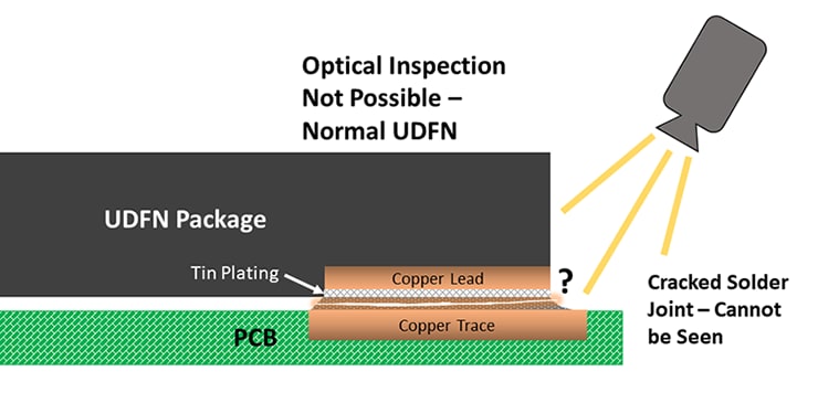
Figure 1: Cracked Solder Joint on Underside of Package
Reap the Benefits of Small Packages Without the Reliability Headaches
To address the need for a reliable, small footprint requirement for serial EEPROMs, we offer a side Wettable Flank (WF) UDFN package that allows for better PCB solder adhesion and improved AOI in identifying defects. The WF package offered for our EEPROMs is a small footprint 8-contact, 2 × 3 × 0.5-mm UDFN package that is well suited for space-constrained applications.
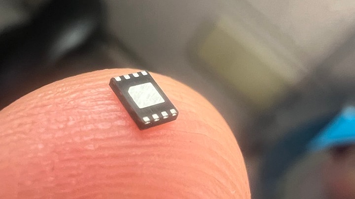
Figure 2: Underside of the WF UDFN Package
Below is a side cut-away view of a standard DFN versus a WF DFN. On a standard DFN, the solder contact resides mostly underneath the package with only exposed copper on the side. Solder usually adheres only to the plated tin on the underside of the solder pad, making it difficult or impossible to detect damaged solder connections using AOI. X-ray inspection can be used to detect hidden, faulty solder joints, but is far more expensive than AOI and is not available on most assembly lines. On the WF package, the solder contact includes a step-cut which extends the tin plating farther up the side of the package. See Figure 3 for an illustration of this step-cut.
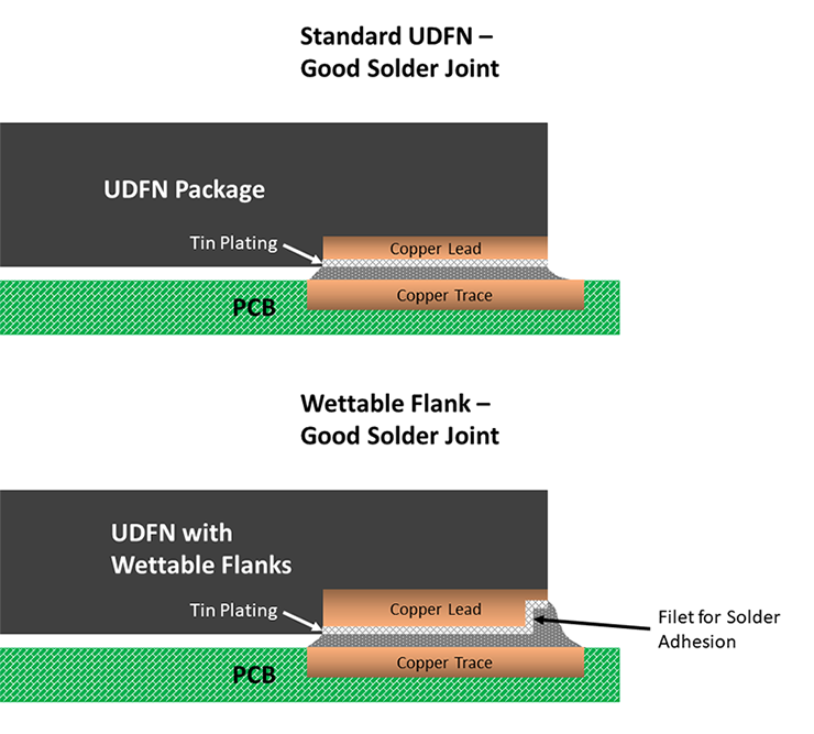
Figure 3: Ideal Solder Connection, Standard DFN vs. WF DFN
This extra tin-plating allows solder to extend up the side of the package to create an easily visible solder joint. The quality of the joint is now easy to evaluate using AOI. Actual images of this joint can be seen below.
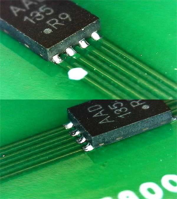
Figure 4: WF DFN Showing Easily Visible Solder Joints
Easily visible solder joints are needed to ensure detection of potentially problematic solder connections made on the assembly line. AOI can more easily detect these types of faulty connections if WF packages are used in place of standard leadless packages.
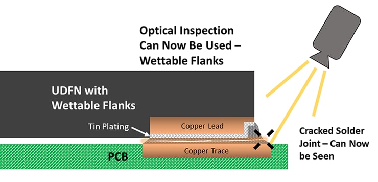
Figure 5: Side Cut-Away View of WF DFN with Cracked Solder Joint
There are different types of faulty solder joints which are more easily detectable using AOI with a WF package, such as cold joints, dry joints or cracked joints.
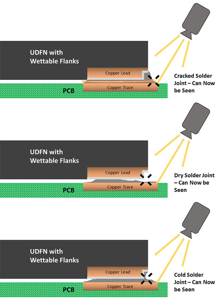
Figure 6: Various Examples of Faulty Solder Joints


