News Centerposition:Baoxingwei > News Center > 正文
SST25VF064C to SST26VF064B/064BA Migration
Edit:Baoxingwei Technology | Time:2023-11-20 15:48 | Number of views:235
1.0 INTRODUCTION
The Serial Quad I/O™ (SQI™) family of flash-memory devices features a six-wire, 4-bit I/O interface that allows for low-power, high-performance operation in a low pin-count package. SST26VF064B/064BA also supports full command-set compatibility to traditional Serial Peripheral Interface (SPI) protocol. This document lists all the firmware and hardware changes required to migrate from SST25VF064C to SST26VF064B/064BA. Refer to the SST26VF064B/ 064BA data sheet (DS20005119) for more information.

1. WSON and WDFN are different designators for the same package 2. TBGA is a new package available for SST26VF064B/064BA
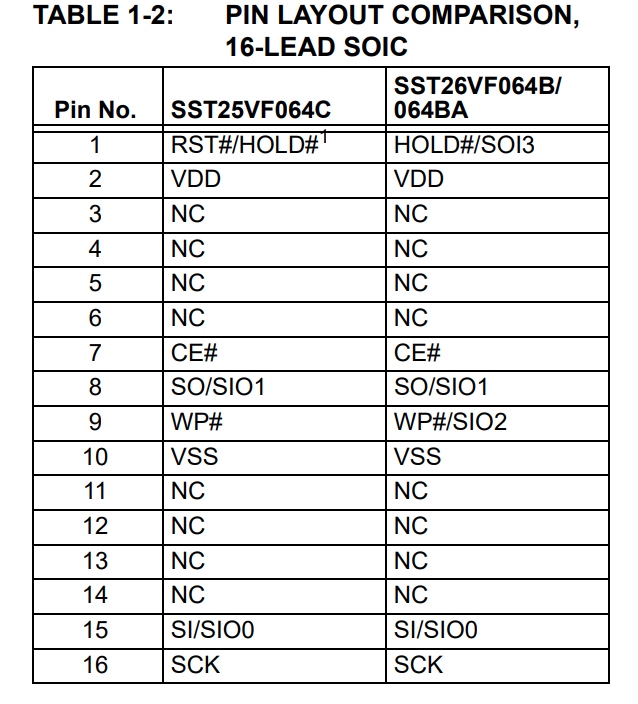
For SST25VF064C, Pin 1 is RST# pin at power-up. For SST26VF064B/064BA, Pin 1 is HOLD# pin at power-up.
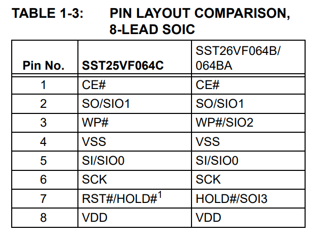
For SST25VF064C, Pin 7 is RST# pin at power-up. For SST26VF064B/064BA, Pin 7 is HOLD# pin at power-up.
2.0 MIGRATION CONSIDERATIONS
The following topics should be considered when migrating from SST25VF064C to SST26VF064B/064BA.
2.1 Reset Pin Function at Power-UpSST25VF064C powers up with the Reset-pin function enabled. Reset-pin function is not supported by SST26VF064B/064BA. SST26VF064B/064BA executes a Reset by software reset using Reset Enable (66H) or Reset memory (99H) software instruction commands.
2.2 Status and Configuration Register
The status register of the SST25VF064C differs from the Status register of SST26VF064B/064BA. Table 2-1 shows the Status register of SST25VF064C and Table 2-2 shows the Status register of SST26VF064B/064BA. SST26VF064B/064BA also has an additional Configuration register used to configure device operations and setup defaults on I/O configuration and Block Protection state, see Table 2-3.
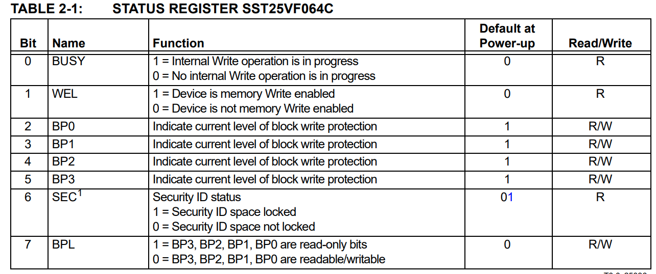
The Security ID status will always be ‘1’ at power-up after a successful execution of the Lockout SID instruction; otherwise, the default at power up is ‘0’
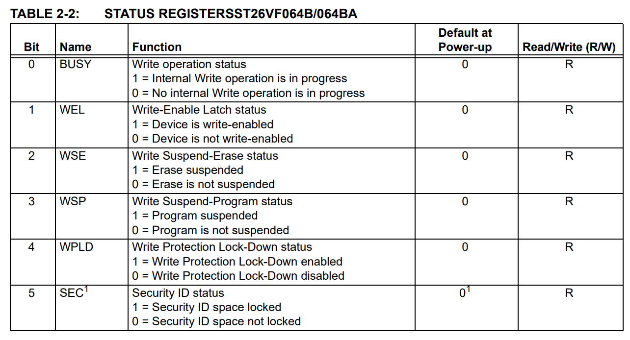

The Security ID status will always be ‘1’ at power-up after a successful execution of the Lockout Security ID instruction, otherwise default at power-up is ‘0’.
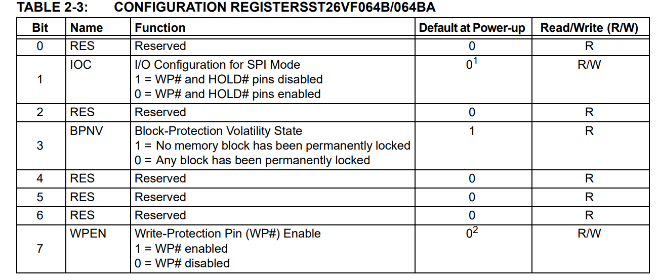
1. SST26VF064B default at Power-up is ‘0’; SST26VF064BA default at Power-up is ‘1’
2. Factory default setting. This is a non-volatile bit; default at power-up will be the setting prior to power-down.
The Read-Status-Register (RDSR) instructions allows the device to read the Status register for SST25VF064C or SST26VF064B/064BA. The Read-ConfigurationRegister (RDCR) enables the device to read the Configuration register for SST26VF064B/064BA.
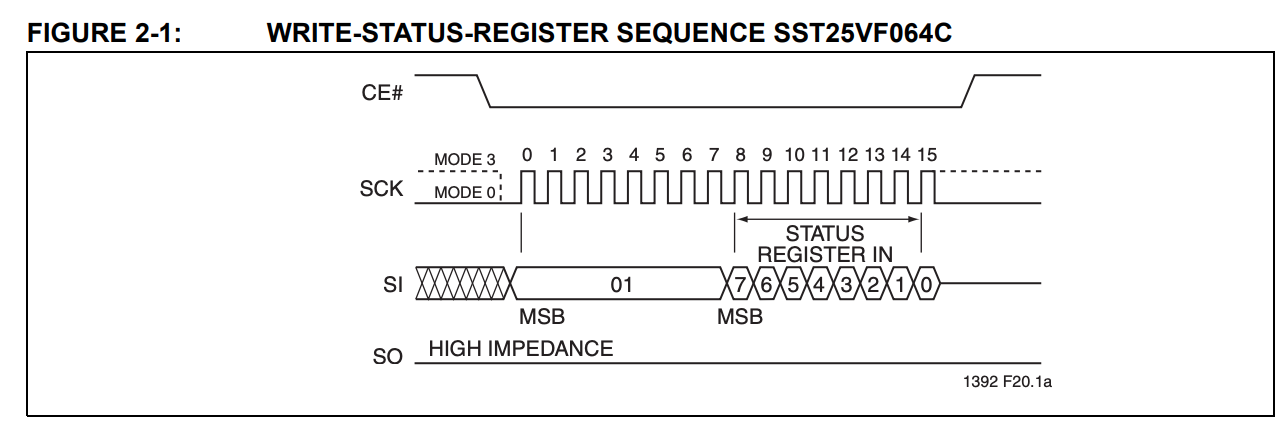
The Write-Status-Register (WRSR) instruction writes to the Status and Configuration registers. Write-Enable (WREN) instruction must be issued prior to WRSR instruction. The WRSR sequence that allows the device to write to the Status register of SST25VF064C is shown in Figure 2-1. The WRSR sequence that allows the device to write to the Status and Configuration registers of SST26VF064B/064BA is shown in Figure 2-2.
The default I/O state factory settings are the same between SST25VF064C and SST26VF064B. The SST26VF064BA factory default setting for I/O WP# and HOLD# are disabled and different from the SST25VF064C.

2.3 Device Protection
SST26VF064B/064BA employs a new protection scheme that allows for more flexibility and a higher level of protection in comparison to the SST25VF064C. SST25VF064C offers traditional memory protection via block protection bits in the Status Register, whereas SST26VF064B/064BA supports individual block protection via Block Protection Register instructions.
Both SST25VF064C and SST26VF064B/064BA power up with memory protected. To execute Program or Erase commands, remove the protection.
To remove the memory protection of SST25VF064C, clear the protection bits in the status register. The status register contains protection bits BP0, BP1, BP2, and BP3, all of which are set to 0 to clear all protection.
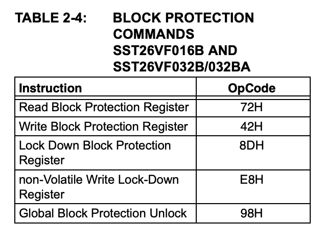
SST26VF064B/064BA supports the Global Block-protection Unlock command (98H) to unlock the entire memory. Table 2-4 lists all block protection commands for SST26VF064B/064BA.
2.4 Device ID
SST25VF064C and SST26VF064B/064BA use different device IDs. The device ID of SST25VF064C is BF254BH. BFH is manufacturer ID, 25H is memory type and 4BH is device ID. The device ID of SST26VF064B/064BA is BF2643H. BFH is manufacturer ID, 26H is memory type and 43H is device ID.
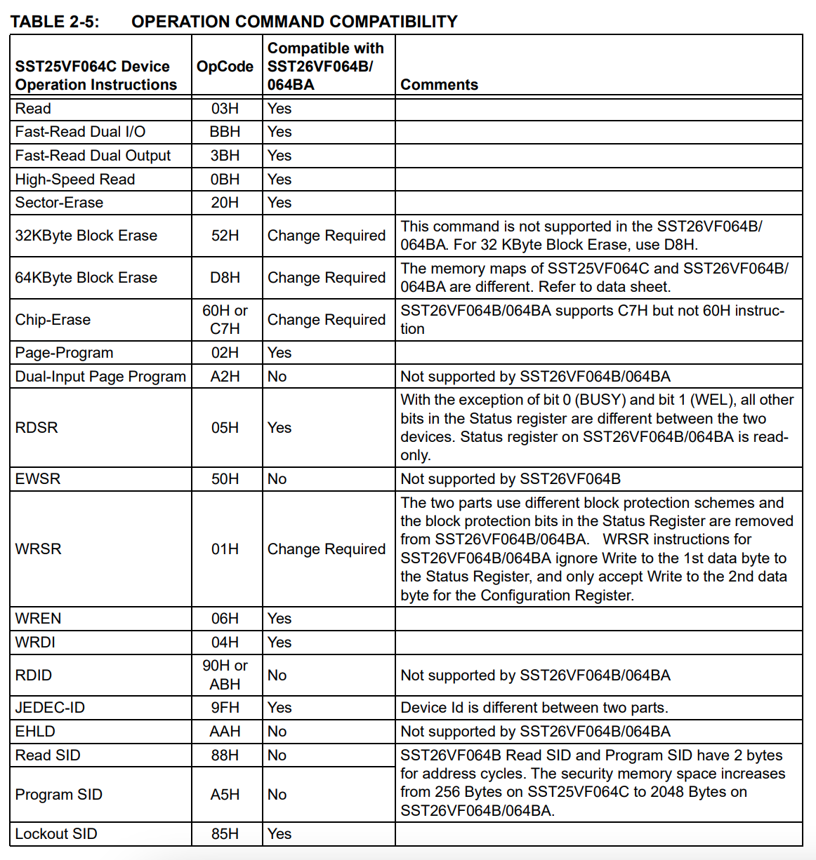
The device IDs for both devices are accessed with the same operation command and protocol, but the returndata will be different for each device. See Table 2-5. for more information about the operation commands.
SST26VF064B/064BA supports JEDEC’s Serial Flash Discoverable Parameters (SFDP) v1.1 as an additional method of device identification.
2.5 Communication Protocol
SST25VF064C only utilizes SPI protocol, but SST26VF064B/064BA can use either SPI and SQI protocol. SST26VF064B/064BA will work with a host controller that only supports SPI. If the host controller supports both SPI and SQI, then all the features of SST26VF064B/064BA are available.
SST25VF064C supports a clock frequency up to 80MHz and SST26VF064B/064BA supports a clock frequency up to 104MHz.
2.6 Host Controller Supports SPI
Most operation commands of SST25VF064C are compatible with SST26VF064B with minimal changes required. See Table 2-5.
2.7 Host Controller Supports Both SPI and SQI
If the host controller can support both SPI and SQI protocol than the above changes described are still relevant and in addition all features of SST26VF064B/064BA are now available for use. A review of the current methods/code to perform read and program must be done and the firmware should be upgraded to take advantage of all the features available as described in the data sheet.
SST26VF064B/064BA supports higher functionality and performance such as:
• up to 104 MHz operating frequency
• multi-I/O read/program capability
• enhanced security and OTP security memory area outside of the main memory array
• JEDEC Serial Flash Discoverable Parameters (SFDP)
• Suspend Program/Erase capability.
Refer to the SST26VF064B/064BA data sheet for detailed instructions.
2.8 Conclusion
This document describes the aspects to consider when migrating from SST25VF064C to SST26VF064B/064BA. SST26VF064B/064BA is a great choice because it supports higher clock frequency, uses both SPI and SQI protocol, and continues to provide the superior reliability represented by SuperFlash® technology.


